

So, where do we go from here?
The future of semiconductors isn’t just about making the chips in your laptop faster. It is about ubiquitous computing.
The trend is moving from General Purpose computing (your PC) to Specialized computing.
- Your toaster will have a chip optimized for heating bread.
- your shoes will have a chip optimized for gait analysis.
- Your glasses will have a chip optimized for overlaying reality.
We are moving toward a world of “Smart Dust”—sensors and processors so small and cheap that they can be sprayed onto crops to monitor moisture or painted onto bridges to detect cracks.
The Edge vs. The Cloud
Right now, most of the thinking happens in the “Cloud” (the massive server farms). You send data to the cloud, it thinks, and sends the answer back.
But with the rise of self-driving cars, you cannot afford the latency (lag) of sending data to the cloud and back. The car needs to react instantly. This requires Edge Computing—putting powerful AI chips inside the car.
We are seeing the migration of supercomputer power from the data center to the device. Your phone, your car, and your drone will become data centers in their own right.
Conclusion: The Never-Ending Revolution
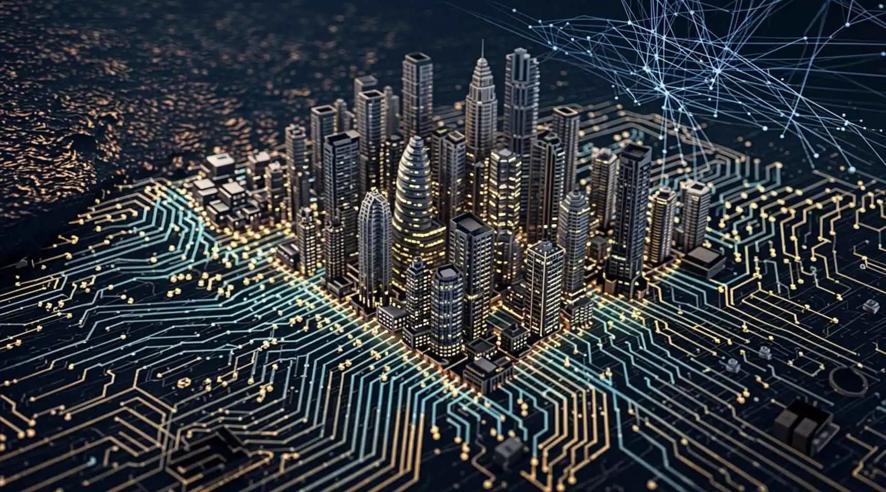
When you look at a silicon chip, you are looking at humanity’s greatest achievement in miniaturization and complexity. It is a city of transistors, printed on a rock.
Semiconductors are the invisible fabric of our lives. They allow us to transcend our biological limitations. They remember what we forget; they calculate what we cannot; they connect us across oceans.
We are currently living through a turning point in history. We are transitioning from the “Information Age” to the “Intelligence Age.” And just as the steam engine defined the Industrial Revolution, the semiconductor defines the Technological Revolution.
The road ahead is fraught with challenges. The physics are getting harder. The geopolitics are getting hotter. The environmental stakes are getting higher.
But the demand for progress is insatiable. We want cures for diseases; we want clean energy; we want to explore the stars. None of it is possible without the chip.
So, the next time you hold your phone, start your car, or chat with an AI, take a moment to appreciate the silent titan inside. Remember that it started as a grain of sand, was doped with impurities, etched with light, and shipped across the world to bring the future to your fingertips.
The Silicon Age is just getting started.
FAQS
Part 1: The Basics & Physics
1.What exactly is a semiconductor?
A semiconductor is a material (usually silicon) that acts as an electrical “fence sitter.” It is neither a good conductor of electricity (like copper) nor a good insulator (like rubber). Its ability to conduct electricity can be controlled, making it perfect for building electronic switches.
- Why is silicon used to make chips?
Silicon is the second most abundant element in the Earth’s crust (after oxygen), making it cheap and readily available. More importantly, it is a semiconductor, meaning it can be easily modified (doped) to control electrical currents.
- What is “doping” in the context of chip manufacturing?
Doping is the process of intentionally adding impurities to pure silicon to change its electrical properties. Adding atoms with extra electrons creates N-type silicon (negative), while adding atoms with “holes” (missing electrons) creates P-type silicon (positive).
- What is a transistor, and why is it important?
A transistor is a tiny switch made by combining N-type and P-type silicon. It controls the flow of electricity. By turning millions or billions of these switches on and off, computers can process binary code (1s and 0s) to perform complex tasks.
- How does a modern chip compare to early computers like ENIAC?
Early computers like ENIAC used vacuum tubes that were large, hot, and unreliable. A modern microchip packs billions of transistors onto a piece of silicon the size of a fingernail, possessing millions of times more computing power than room-sized computers from the 1940s.
Part 2: Manufacturing & Supply Chain
6.What is the difference between a Fabless company and a Foundry?
A Fabless company (like Apple or NVIDIA) designs the chips but does not have factories to manufacture them. A Foundry (like TSMC) is the factory that takes the designs and physically manufactures the silicon wafers.
- Why are semiconductor factories (Fabs) so clean?
Because the features on a chip are microscopic (measured in nanometers), a single speck of dust can ruin an entire circuit. Fabs are hermetically sealed environments with air filtration systems that make the air thousands of times cleaner than the outside world.
- What is lithography?
Lithography is the process of using light to print a circuit pattern onto a silicon wafer. It works similarly to photography, where a mask (the blueprint) blocks light in certain areas to etch the design onto the photoresist-coated wafer.
- Who is ASML, and why are they important?
ASML is a Dutch company that is the sole supplier of the world’s most advanced lithography machines (EUV machines). These machines cost over $200 million each and use extreme ultraviolet light to print the tiniest, most advanced transistors.
- What is a silicon wafer?
A silicon wafer is a thin slice of purified silicon crystal, cut from a long cylindrical ingot. It serves as the base material onto which circuits are built. Wafers are usually round, though the chips cut from them are rectangular or square.
Part 3: Moore’s Law & Technology
- What is Moore’s Law?
Moore’s Law is the observation made by Gordon Moore that the number of transistors on a microchip doubles about every two years, while the cost of computers is halved. It has driven the rapid pace of technological advancement for decades.
- Is Moore’s Law dead?
It is slowing down. As transistors approach the size of atoms, we are hitting physical limits (like quantum tunneling) that make shrinking them difficult. The industry is now shifting to new methods like 3D stacking and chiplets to continue improving performance.
- What is quantum tunneling?
Quantum tunneling is a phenomenon where electrons pass through barriers they shouldn’t be able to cross. In extremely tiny transistors, this causes electrical current to leak uncontrollably, generating heat and errors, which is a major hurdle for continuing to shrink chips.
- How is the industry solving the end of Moore’s Law?
Instead of just shrinking chips (2D), manufacturers are building them upward (3D Stacking). They are also using “chiplets”—smaller, specialized chips connected together—to improve performance and yield without needing to make one massive, perfect chip.
- What is the difference between a CPU and a GPU?
A CPU (Central Processing Unit) has a few powerful cores designed for sequential tasks (like running an operating system). A GPU (Graphics Processing Unit) has thousands of smaller cores designed for parallel tasks (doing many simple calculations at once), making it ideal for graphics and AI.
Part 4: Geopolitics & Economy
- Why are semiconductors called the “new oil”?
Just as oil was the strategic resource that powered the 20th century, semiconductors are the strategic resource powering the 21st century. They are essential for the economy, national defense, and technological leadership, making control over their supply a matter of national security.
- Why is Taiwan so critical to the chip industry?
Taiwan is home to TSMC, which manufactures approximately 90% of the world’s most advanced processing chips. This concentration of manufacturing makes Taiwan the most vulnerable and vital link in the global tech supply chain.
- What is the US CHIPS Act?
The CHIPS and Science Act is a US law passed to subsidize the construction of semiconductor factories (“Fabs”) on American soil. It aims to reduce reliance on foreign manufacturing and strengthen national security.
- How does the chip war affect China?
The US and its allies have restricted the export of advanced chip-making equipment (like ASML machines) and high-end chips to China. This forces China to invest heavily in building its own self-sufficient domestic semiconductor supply chain to bypass sanctions.
- What would happen if the global chip supply stopped?
A halt in chip production would cause a global economic collapse. The manufacturing of cars, medical devices, servers, defense systems, and consumer electronics would stop, potentially costing the global economy over $1 trillion in a single year.
Part 5: Future, AI & Environment
- Why are GPUs essential for Artificial Intelligence (AI)?
Training AI requires processing massive datasets simultaneously. The parallel processing power of GPUs (doing thousands of math problems at once) is perfectly suited for this, making them the “engine” of the current AI boom.
- What are Silicon Carbide (SiC) and Gallium Nitride (GaN)?
These are Compound Semiconductors that outperform pure silicon in high-power and high-frequency applications. SiC is crucial for Electric Vehicles (efficiency/range), while GaN is used in fast chargers and 5G/6G networks.
- What is Silicon Photonics?
Silicon Photonics is a technology that uses light (photons) instead of electricity (electrons) to transmit data within a chip. It promises to make data transfer much faster and more energy-efficient, helping solve the heat and speed limits of modern computing.
- What is the environmental impact of chip manufacturing?
Chip manufacturing is resource-intensive, consuming millions of gallons of water per day for cleaning wafers and massive amounts of electricity. It also involves toxic chemicals that require careful disposal.
- What is Edge Computing?
Edge Computing involves processing data locally on the device (like a self-driving car or smart sensor) rather than sending it to a central cloud server. This reduces latency (lag) and requires powerful, specialized chips to be placed at the “edge” of the network.
Disclaimer: The content on this blog is for informational purposes only. Author’s opinions are personal and not endorsed. Efforts are made to provide accurate information, but completeness, accuracy, or reliability are not guaranteed. Author is not liable for any loss or damage resulting from the use of this blog. It is recommended to use information on this blog at your own terms.